Search icon CANCEL
Subscription
0
Cart icon
Your Cart (0 item)
Close icon
You have no products in your basket yet
Arrow left icon
Explore Products
Best Sellers
New Releases
Books
Videos
Audiobooks
Learning Hub
Free Learning
Arrow right icon
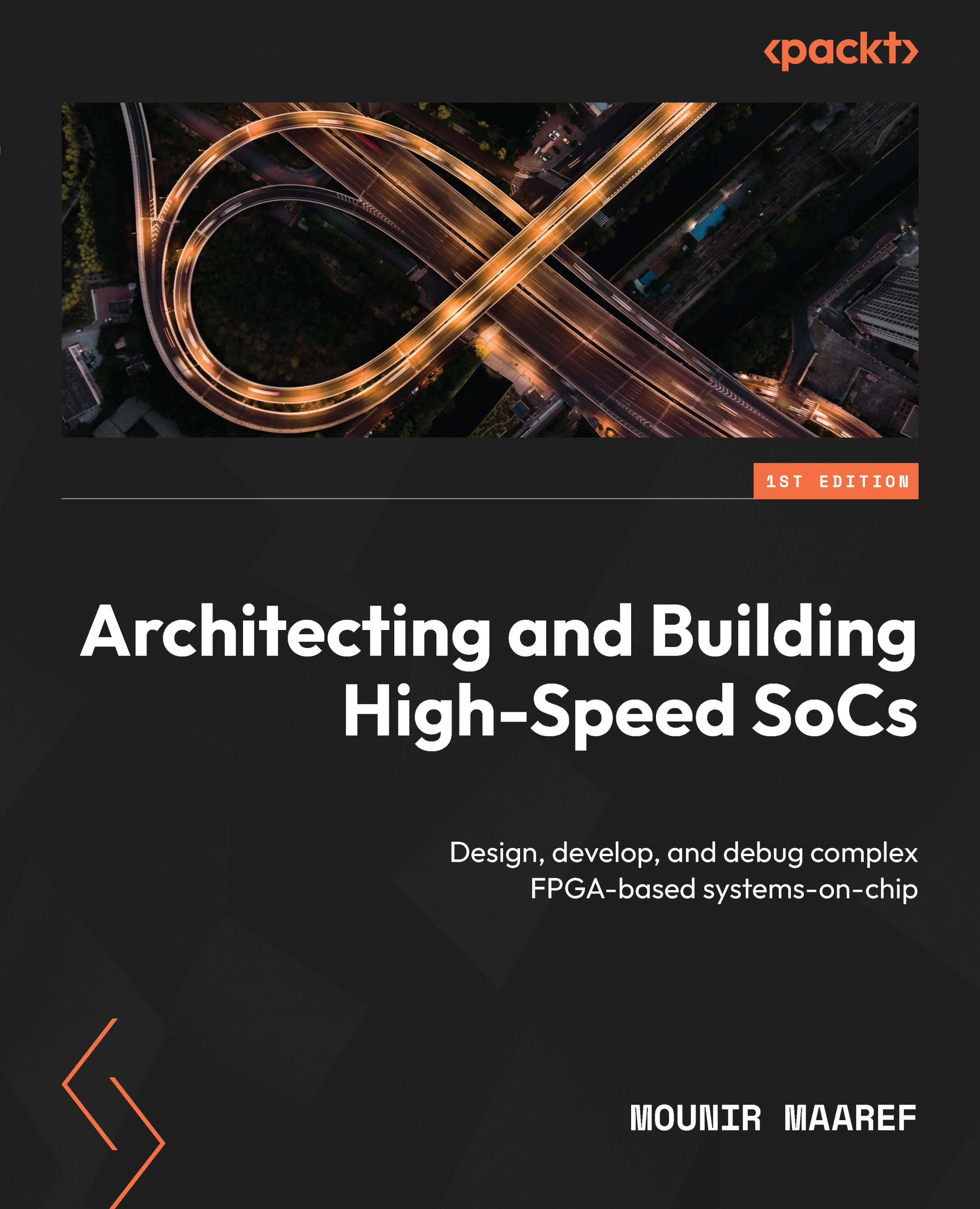
Architecting and Building High-Speed SoCs

Architecting and Building High-Speed SoCs: Design, develop, and debug complex FPGA based systems-on-chip

eBook
$9.99 $37.99
Paperback
$46.99
Subscription
Free Trial
Renews at $19.99p/m

What do you get with eBook?

Product feature icon Instant access to your Digital eBook purchase
Product feature icon Download this book in EPUB and PDF formats
Product feature icon Access this title in our online reader with advanced features
Product feature icon DRM FREE - Read whenever, wherever and however you want
Product feature icon AI Assistant (beta) to help accelerate your learning
OR
Modal Close icon
Payment Processing...
tick Completed

Billing Address

Table of content icon View table of contents Preview book icon Preview Book

Architecting and Building High-Speed SoCs

Introducing FPGA Devices and SoCs

In this chapter, we will begin by describing what the field-programmable gate array (FPGA) technology is and its evolution since it was first invented by Xilinx in the 1980s. We will cover the electronics industry gap that FPGA devices cover, their adoption, and their ease of use for implementing custom digital hardware functions and systems. Then, we will describe the high-speed FPGA-based system-on-a-chip (SoC) and its evolution since it was introduced as a solution by the major FPGA vendors in the early 2000s. Finally, we will look at how various applications classify SoCs, specifically for FPGA implementations.

In this chapter, we’re going to cover the following main topics:

  • Xilinx FPGA devices overview
  • Xilinx SoC overview and history
  • Xilinx Zynq-7000 SoC family hardware features
  • Xilinx Zynq UltraScale+ MPSoC family hardware features
  • SoC in ASIC technologies

Xilinx FPGA devices overview

An FPGA is a very large-scale integration (VLSI) integrated circuit (IC) that can contain hundreds of thousands of configurable logic blocks (CLBs), tens of thousands of predefined hardware functional blocks, hundreds of predefined external interfaces, thousands of memory blocks, thousands of input/output (I/O) pads, and even a fully predefined SoC centered around an IBM PowerPC or an ARM Cortex-A class processor in certain FPGA families. These functional elements are optimally spread around the FPGA silicon area and can be interconnected via programmable routing resources. This allows them to behave in a functional manner that’s desired by a logic designer so that they can meet certain design specifications and product requirements.

Application-specific integrated circuits (ASICs) and application-specific standard products (ASSPs) are VLSI devices that have been architected, designed, and implemented for a given product or a particular application domain. In contrast to ASICs and ASSPs, FPGA devices are generic ICs that can be programmed to be used in many applications and industries. FPGAs are usually reprogrammable as they are based on static random-access memory (SRAM) technology, but there is a type that is only programmed once: one-time programmable (OTP) FPGAs. Standard SRAM-based FPGAs can be reprogrammed as their design evolves or changes, even once they have been populated in the electronics design board and after being deployed in the field. The following diagram illustrates the concept of an FPGA IC:

Figure 1.1 – FPGA IC conceptual diagram

Figure 1.1 – FPGA IC conceptual diagram

As we can see, the FPGA device is structured as a pool of resources that the design assembles to perform a given logical task.

Once the FPGA’s design has been finalized, a corresponding configuration binary file is generated to program the FPGA device. This is typically done directly from the host machine at development and verification time over JTAG. Alternatively, the configuration file can be stored in a non-volatile media on the electronics board and used to program the FPGA at powerup.

A brief historical overview

Xilinx shipped its first FPGA in 1985 and its first device was the XC2064; it offered 800 gates and was produced on a 2.0μ process. The Virtex UltraScale+ FPGAs, some of the latest Xilinx devices, are produced in a 14nm process node and offer high performance and a dense integration capability. Some modern FPGAs use 3D ICs stacked silicon interconnect (SSI) technology to work around the limitations of Moore’s law and pack multiple dies within the same package. Consequently, they now provide an immense 9 million system logic cells in a single FPGA device, a four order of magnitude increase in capacity alone compared to the first FPGA; that is, XC2064. Modern FPGAs have also evolved in terms of their functionality, higher external interface bandwidth, and a vast choice of supported I/O standards. Since their initial inception, the industry has seen a multitude of quantitative and qualitative advances in FPGA devices’ performance, density, and integrated functionalities. Also, the adoption of the technology has seen a major evolution, which has been aided by adequate pricing and Moore’s law advancements. These breakthroughs, combined with matching advances in software development tools, intellectual property (IP), and support technologies, have created a revolution in logic design that has also penetrated the SoC segment.

There has also been the emergence of the new Xilinx Versal devices portfolio, which targets the data center’s workload acceleration and offers a new AI-oriented architecture. This device class family is outside the scope of this book.

FPGA devices and penetrated vertical markets

FPGAs were initially used as the electronics board glue logic of digital devices. They were used to implement buses, decode functions, and patch minor issues discovered in the board ASICs post-production. This was due to their limited capacities and functionalities. Today’s FPGAs can be used as the hearts of smart systems and are designed with their full capacities in terms of parallel processing and their flexible adaptability to emerging and changing standards, specifically at the higher layers, such as the Link and Transactions layers of new communication or interface protocols. These make reconfiguring FPGA the obvious choice in medium or even large deployments of these emerging systems. With the addition of ASIC class embedded processing platforms within the FPGA for integrating a full SoC, FPGA applications have expanded even deeper into industry verticals where it has seen limited useability in the past. It is also very clear that, with the prohibitive cost of non-recurring engineering (NRE) and producing ASICs at the current process nodes, FPGAs are becoming the first choice for certain applications. They also offer a very short time to market for certain segments where such a factor is critical for the product’s success.

FPGAs can be found across the board in the high-tech sector and range from the classical fields such as wired and wireless communication, networking, defense, aerospace, industrial, audio-video broadcast (AVB), ASIC prototyping, instrumentation, and medical verticals to the modern era of ADAS, data centers, the cloud and edge computing, high-performance computing (HPC), and ASIC emulation simulators. They have an appealing reason to be used almost everywhere in an electronics-based application.

An overview of the Xilinx FPGA device families

Xilinx provides a comprehensive portfolio of FPGA devices to address different system design requirements across a wide range of the application’s spectrum. For example, Xilinx FPGA devices can help system designers construct a base platform for a high-performance networking application necessitating a very dense logic capacity, a very wide bandwidth, and performance. They can also be used for low-cost, small-footprint logic design applications using one of the low-cost FPGA devices either for high or low-volume end applications.

In this large offering, there are the cost-optimized families such as the Spartan-7 family and the Spartan-6 family, which are built using a 45nm process node, the Artix-7 family, and the Zynq-7000 family, which is built using a 28nm process node.

There is also the 7-series family in a 28nm process, which includes the Artix-7, Kintex-7, and Virtex-7 families of FPGAs, in addition to the Spartan-7 family.

Additionally, there are FPGAs from the UltraScale Kintex and Virtex families in a 20nm process node.

The UltraScale+ category contains three more additional families – the Artix UltraScale+, the Kintex UltraScale+, and the Virtex UltraScale+, all in a 16nm process node.

Each device family has a matrixial offering table that is defined by the density of logic, the number of functional hardware blocks, the capacity of the internal memory blocks, and the amount of I/Os in each package. This makes the offered combinations an interesting catalog to pick a device that meets the requirements of the system to build using the specific FPGA. To examine a given device offering matrix, you need to consult the specific FPGA family product table and product selection guide. For example, for the UltraScale+ FPGAs, please go to https://www.xilinx.com/content/dam/xilinx/support/documentation/selection-guides/ultrascale-plus-fpga-product-selection-guide.pdf.

An overview of the Xilinx FPGA devices features

As highlighted in the introduction to this chapter, modern Xilinx FPGA devices contain a vast list of hardware block features and external interfaces that relatively define their category or family and, consequently, make them suitable for a certain application or a specific market vertical. This chapter looks at the rich list of these features to help you understand what today’s FPGAs are capable of offering system designers. It is worth noting that not all the FPGAs contain all these elements.

For a detailed overview of these features, you are encouraged to examine the Xilinx UltraScale+ Data Sheet as a good starting point at https://www.xilinx.com/content/dam/xilinx/support/documentation/data_sheets/ds890-ultrascale-overview.pdf.

In the following subsections, we will summarize some of these features.

Logic elements

Modern Xilinx FPGAs have an abundance of CLBs. These CLBs are formed by lookup tables (LUTs) and registers known as flip-flops. These CLBs are the elementary ingredients that logic user functions are built from to form the desired engine to perform a combinatorial function that’s coupled (or not) with sequential logic. These are also built from Flip-Flop resources contained within the CLBs. Following a full design process from design capture, to synthesizing and implementing the production of a binary image to program the FPGA device, these CLBs are configured to operate in a manner that matches the aforementioned required partial task within the desired function defined by the user. The CLB can also be configured to behave as a deep shift register, a multiplexer, or a carry logic function. It can also be configured as distributed memory from which more SRAM memory is synthesized to complement the SRAM resources that can be built using the FPGA device block’s RAM.

Storage

Xilinx FPGAs have many block RAMs with built-in FIFO. Additionally, in UltraScale+ devices, there are 4Kx72 UltraRAM blocks. As mentioned previously, the CLB can also be configured as distributed memory from which more SRAM memory can be synthesized.

The Virtex UltraScale+ HBM FPGAs can integrate up to 16 GB of high-bandwidth memory (HBM) Gen2.

Xilinx Zynq UltraScale+ MPSoC also provides many layers of SRAM memory within its ARM-based SoC, such as OCM memory and the Level 1 and Level 2 caches of the integrated CPUs and GPUs.

Signal processing

Xilinx FPGAs are rich in resources for digital signal processing (DSP). They have DSP slices with 27x18 multipliers and rich local interconnects. The DSP slice has many usage possibilities, as described in the FPGA datasheet.

Routing and SSI

The Xilinx FPGA’s device interconnect employs a routing infrastructure, which is a combination of configurable switches and nets. These allow the FPGA elements such as the I/O blocks, the DSP slices, the memories, and the CLBs to be interconnected.

The efficiency of using these routing resources is as important as the device hardware’s logical resources and features. This is because they represent the nerve system of the FPGA device, their abundance of interconnect logic, and their functional elements, which are crucial to meeting the design performance criteria.

Design clocking

Xilinx FPGA devices contain many clock management elements, including digital local loops (DLLs) for clock generation and synthesis, global buffers for clock signal buffering, and routing infrastructure to meet the demands of many challenging design requirements. The flexibility of the clocking network minimizes the inter-signal delays or skews.

External memory interfaces

The Xilinx FPGAs can interface to many external parallel memories, including DDR4 SDRAM. Some FPGAs also support interfacing to external serial memories, such as Hybrid Memory Cube (HMC).

External interfaces

Xilinx FPGA devices interface to the external ICs through I/Os that support many standards and PHY protocols, including the serial multi-gigabit transceivers (MGTs), Ethernet, PCIe, and Interlaken.

ARM-based processing subsystem

The first device family that Xilinx brought to the market that integrated an ARM CPU was the Zynq-7000 SoC FPGA with its integrated ARM Cortex-A9 CPU. This family was followed by the Xilinx Zynq UltraScale+ MPSoCs and RFSoCs, which feature a processing system (PS) that includes a dual or a quad-core variant of the ARM Cortex-A53, and a dual-core ARM Cortex-R5F. Some variants have a graphics processing unit (GPU). We will delve into the Xilinx SoCs in the next chapter.

Configuration and system monitoring

Being SRAM-based, the FPGA requires a configuration file to be loaded when powered up to define its functionality. Consequently, any errors that are encountered in the FPGA’s configuration binary image, either at configuration time or because of a physical problem in mission mode, will alter the overall system functionality and may even cause a disastrous outcome for sensitive applications. Therefore, it is a necessity for critical applications to have system monitoring to urgently intervene when such an error is discovered to correct it and limit any potential damage via its built-in self-monitoring mechanism.

Encryption

Modern FPGAs provide decryption blocks to address security needs and protect the device’s hardware from hacking. FPGAs with integrated SoC and PS blocks have a configuration and security unit (CSU) that allows the device to be booted and configured safely.

Xilinx SoC overview and history

In the early 2000s, Xilinx introduced the concept of building embedded processors into its available FPGAs at the time, namely the Spartan-2, Virtex-II, and Virtex-II Pro families. Xilinx brought two flavors of these early SoCs to the market: a soft version and an initial hard macro-based option in the Virtex-II Pro FPGAs.

The soft flavor uses MicroBlaze, a Xilinx RISC 32-bit based soft processor coupled initially with an IBM-based bus infrastructure called CoreConnect and a rich set of peripherals, such as a Gigabits Ethernet MACs, PCIe, and DDR DRAM, just to name a few. A typical MicroBlaze soft processor-based SoC looks as follows:

Figure 1.2 – Legacy FPGA MicroBlaze embedded system

Figure 1.2 – Legacy FPGA MicroBlaze embedded system

The hard macro version uses a 32-bit IBM PowerPC 405 processor. It includes the CPU core, a memory management unit (MMU), 16 KB L1 data and 16 KB L1 instruction caches, timer resources, the necessary debug and trace interfaces, the CPU CoreConnect-based interfaces, and a fast memory interface known as on-chip memory (OCM). The OCM connects to a mapped region of internal SRAM that’s been built using the FPGA block RAMs for fast code and data access. The following diagram shows a PowerPC 405 embedded system in a Virtex-II Pro FPGA device:

Figure 1.3 – Virtex-II Pro PowerPC405 embedded system

Figure 1.3 – Virtex-II Pro PowerPC405 embedded system

Embedded processing within FPGAs has received a wide adoption from different vertical spaces and opened the path to many single-chip applications that previously required the use of an external CPU, alongside the FPGA device, as the main board processor.

The Virtex-4 FX was the next generation to include the IBM PowerPC 405 and improved its core speed.

The Virtex-5 FXT followed and integrated the IBM PowerPC 440x5 CPU, a dual-issue superscalar 32-bit embedded processor with an MMU, a 32 KB instruction cache, a 32 KB data cache, and a Crossbar interconnect. To interface with the rest of the FPGA logic, it has a processor local bus (PLB) interface, an auxiliary processor unit (APU) for connecting FPU, and a custom coprocessor built into the FPAG logic. It also has a high-speed memory controller interface. With the Ethernet Tri-Speed 10/100/1000 MACs integrated as hardware functional blocks in the FPGA, we started seeing the main ingredients necessary for making an SoC in FPGAs, with most of the logic-consuming hardware functions now bundled together around the CPU block or delivered as a hardware functional block that just needs interfacing and connecting to the CPU. This was a step close to a full SoC in FPGAs. The following diagram shows a PowerPC 440 embedded system in a Virtex-5 FXT FPGA device:

Figure 1.4 – Virtex-5 FXT PowerPC440 embedded system

Figure 1.4 – Virtex-5 FXT PowerPC440 embedded system

The Virtex-5 FXT was the last Xilinx FPGA to include an IBM-based CPU; the future was switching to ARM and providing a full SoC in FPGAs with the possibility to interface to the FPGA logic through adequate ports. This offered the industry a new kind of SoC that, within the same device, combined the power of an ASIC and the programmability of the Xilinx-rich FPGAs. This brings us to this book’s main topic, where we will delve into and try to deal with all Xilinx’s related design development and technological aspects while taking an easy-to-follow and progressive approach.

The following diagram illustrates the approach taken by Xilinx to couple an ARM-based CPU SoC with the Xilinx FPGA logic in the same chip:

Figure 1.5 – Zynq-7000 SoC FPGA conceptual diagram

Figure 1.5 – Zynq-7000 SoC FPGA conceptual diagram

A short survey of the Xilinx SoC FPGAs based on an ARM CPU

The first device family that Xilinx brought to the market for integrating an ARM Cortex-A9 CPU was the Zynq-7000 FPGA. The Cortex-A9 is a 32-bit processor that implements the ARMv7-A architecture and can run many instruction formats. These are available in two configurations: a single Cortex-A9 core in the Zynq-7000S devices and a dual Cortex-A9 cluster in the Zynq-7000 devices.

The next generation that followed was the Zynq UltraScale+ MPSoC devices, which provide a 64-bit ARM CPU cluster for integrating an ARM Cortex-A53, coupled with a 32-bit ARM Cortex-R5 in the same SoC. The Cortex-A53 CPU implements the ARMv8-A architecture, while the Cortex-R5 implements the ARMv7 architecture and, specifically, the R profile. The Zynq UltraScale+ MPSoC comes in different configurations. There is the CG series with a dual-core Cortex-A53 cluster, the EG series with a quad-core Cortex-A53 cluster and an ARM MALI GPU, and the EV series, which comes with additional video codecs to what is available in the EG series.

A few years ago, Xilinx also launched a version of the MPSoC with key components to help build advanced radio connectivity SoCs: the Zynq UltraScale+ RFSoC.

Xilinx Zynq-7000 SoC family hardware features

As mentioned previously, the Zynq FPGA SoC integrates a popular ARM CPU based on the ARMv7, and the classical FPGA part based on the Xilinx 7th generation logic with rich hardware features.

For a detailed description of the Zynq-7000 SoC FPGA and its features, please refer to the SoC Technical Reference Manual (TRM) available at https://www.xilinx.com/support/documentation/user_guides/ug585-Zynq-7000-TRM.pdf.

This section specifies the main Zynq-7000 SoC features and defines them to help you quickly visualize the device’s capabilities.

The SoC is mainly composed of an application processor unit (APU), a connectivity matrix, an OCM memory interface, external memory interfaces, and the I/O peripherals (IOP) block.

The following diagram provides a detailed architectural view of the Zynq-7000 SoC:

Figure 1.6 – Zynq-7000 SoC architecture – dual-core cluster example

Figure 1.6 – Zynq-7000 SoC architecture – dual-core cluster example

Zynq-7000 SoC APU

The CPU cluster topology is built around an ARM Cortex-A9 CPU, which comes in a dual-core or a single-core MPCore. Each CPU core has an L1 instruction cache and an L1 data cache. It also has its own MMU, a floating-point unit (FPU), and a NEON SIMD engine. The CPU cluster has an L2 common cache and a snoop control unit (SCU). This SCU provides an accelerator coherency port (ACP) that extends cache coherency beyond the cluster with external masters when implemented in the FPGA logic.

Each core provides a performance figure of 2.5 DMIPS/MHz with an operating frequency ranging from 667 MHz to 1 GHz, depending on the Zynq FPGA speed grade. The FPU supports both single and double precision operands with a performance figure of 2.0 MFLOPS/MHz. The CPU core is TrustZone-enabled for secure operation. It supports code compression via the Thumb-2 instructions set. The Level 1 instructions and data caches are both 32 KB in size and are 4-way set-associative.

The CPU cluster supports both SMP and AMP operation modes. The Level 2 cache is 512 KB in size and is common to both CPU cores and for both instructions and data. The L2 cache is an eight-way set associative. The cluster also has a 256 KB OCM RAM that can be accessed by the APU and the programmable logic (PL).

The PS has 8-channel DMA engines that support transactions between memories, peripherals, and scatter-gather operations. Their interfaces are based on the AXI protocol. The FPGA PL can use up to four DMA channels.

The SoC has a general interrupt controller (GIC) version 1.0 (GIC v1). The GIC distributes interrupts to the CPU cluster cores according to the user’s configuration and provides support for priority and preemption.

The PS supports debugging and tracing and is based on ARM CoreSight interface technology.

Zynq-7000 SoC memory controllers

The Zynq device supports both SDRAM DDR memory and static memories. DDR3/3L/2 and LPDDR2 speeds are supported. The static memory controllers interface to QSPI flash, NAND, and parallel NOR flash.

The SDRAM DDR interface

The SDRAM DDR interface has a dedicated 1 GB of system address space. It can be configured to interface to a full-width 32-bit wide memory or a half-width 16-bit wide memory. It provides support for many DDR protocols. The PS also includes the DDR PHY and can operate at many speeds – up to a maximum of 1,333 Mb/s. This is a multi-port controller that can share the SDRAM DDR memory bandwidth with many SoC clients within the PS or PL regions over four ports. The CPU cluster is connected to a port; two ports serve the PL, while the fourth port is exposed to the SoC central switches, making access possible to all the connected masters.

The following diagram is a memory-centric representation of the SDRAM DDR interface of the Zynq-7000 SoC:

Figure 1.7 – Zynq-7000 SoC DDR SDRAM memory controller

Figure 1.7 – Zynq-7000 SoC DDR SDRAM memory controller

Static memory interfaces

The static memory controller (SMC) is based on ARM’s PL353 IP. It can interface to NAND flash, SRAM, or NOR flash memories. It can be configured through an APB interface via its operational registers. The SMC supports the following external static memories:

  • 64 MB of SRAM in 8-bit width
  • 64 MB of parallel NOR flash in 8-bit width
  • NAND flash

The following diagram provides a micro-architectural view of the Zynq-7000 SoC SMC:

Figure 1.8 – Zynq-7000 SoC static memory controller architecture

Figure 1.8 – Zynq-7000 SoC static memory controller architecture

QSPI flash controller

The IOP block of the Zynq-7000 SoC includes a QSPI flash interface. It supports serial flash memory devices, as well as three modes of operation: linear addressing mode, I/O mode, and legacy SPI mode.

The software implements the flash device protocol in I/O mode. It provides the commands and data to the controller using the interface registers and reads the received data from the flash memory via the flash registers.

In linear addressing mode, the controller maps the flash address space onto the AXI address space and acts as a translation block between them. Requests that are received on the AXI port of the QSPI controller are converted into the necessary commands and data phases, while read data is put on the AXI bus when it’s received from the flash memory device.

In legacy mode, the QSPI interface behaves just like an ordinary SPI controller.

To write the software drivers for a given flash device to control via the Zynq-7000 SoC QSPI controller, you should refer to both the flash device data sheet from the flash vendor and the QSPI controller operational mode settings detailed in the Zynq-7000 TRM. The URL for this was mentioned at the beginning of this section.

The QPSI controller supports multiple flash device arrangements, such as 8-bit access using two parallel devices (to double the device throughput) or a 4-bit dual rank (to increase the memory capacity).

Zynq-7000 I/O peripherals block

The IOP block contains the external communication interfaces and includes two tri-mode (10/100/1 GB) Ethernet MACs, two USB 2.0 OTG peripherals, two full CAN bus interfaces, two SDIO controllers, two full-duplex SPI ports, two high-speed UARTs, and two master and slave I2C interfaces. It also includes four 32-bit banks GPIO. The IOP can interface externally through 54 flexible multiplexed I/Os (MIOs).

Zynq-7000 SoC interconnect

The interconnect is ARM AMBA AXI-based with QoS support. It groups masters and slaves from the PS and extends the connectivity to PL-implemented masters and slaves. Multiple outstanding transactions are supported. Through the Cortex-A9 ACP ports, I/O coherency is possible so that external masters and the CPU cores can coherently share data, minimizing the CPU core cache management operations. The interconnect topology is formed by many switches based on ARM NIC-301 interconnect and AMBA-3 ports. The following diagram provides an overview of the Zynq-7000 SoC interconnect:

Figure 1.9 – Zynq-7000 SoC interconnect topology

Figure 1.9 – Zynq-7000 SoC interconnect topology

Xilinx Zynq Ultrascale+ MPSoC family overview

The Zynq UltraScale+ MPSoC is the second generation of the Xilinx SoC FPGAs based on the ARM CPU architecture. Like its predecessor, the Zynq-7000 SoC, it is based on the approach of combining the FPGA logic HW configurability and the SW programmability of its ARM CPUs but with improvements in both the FPGA logic and the ARM processor CPUs, as well as its PS features. The UltraScale+ MPSoC offers a heterogeneous topology that couples a powerful 64-bit application processor (implementing the ARMv8-A architecture) and a 32-bit real-time R-profile processor.

The PS includes many types of processing elements: an APU, such as the dual-core or quad-core Cortex-A53 cluster, the dual-core Cortex-R5F real-time processing unit (RPU), the Mali GPU, a PMU, and a video codec unit (VCU) in the EG series. The PS has an efficient power management scheme due to its granular power domains control and gated power islands. The Zynq UltraScale+ MPSoC has a configurable system interconnect and offers the user overall flexibility to meet many application requirements. The following diagram provides an architectural view of the Zynq UltraScale+ SoC:

Figure 1.10 – Zynq UltraScale+ MPSoC architecture – quad-core cluster

Figure 1.10 – Zynq UltraScale+ MPSoC architecture – quad-core cluster

The following section provides a brief description of the main features of the Zynq UltraScale+ MPSoC. For a detailed technical description, please read the Zynq UltraScale+ MPSoC TRM at https://www.xilinx.com/support/documentation/user_guides/ug1085-zynq-ultrascale-trm.pdf.

Zynq UltraScale+ MPSoC APU

The CPU cluster topology is built around an ARM Cortex-A53 CPU, which comes in a quad-core or a dual-core MPCore. The CPU cores implement the Armv8-A architecture with support for the A64 instruction set in AArh64 or the A32/T32 instruction set in AArch32. Each CPU core comes with an L1 instruction cache with parity protection and an L1 data cache with ECC protection. The L1 instruction cache is 2-way set-associative, while the L1 data cache is 4-way set-associative. It also has its own MMU, an FPU, and a Neon SIMD engine. The CPU cluster has a 16-way set-associative L2 common cache and an SCU with an ACP port that extends cache coherency beyond the cluster with external masters in the PL. Each CPU core provides a performance figure of 2.3 DMIPS/MHz with an operating frequency of up to 1.5 GHz. The CPU core is also TrustZone enabled for secure operations.

The CPU cluster can operate in symmetric SMP and asymmetric AMP modes with the power island gating for each processor core. Its unified Level 2 cache is ECC protected, is 1 MB in size, and is common to all CPU cores and both instructions and data.

The APU has a 128-bit AXI coherent extension (ACE) port that connects to the PS cache coherent interconnect (CCI), which is associated with the system memory management unit (SMMU). The APU has an ACP slave port that allows the PL master to coherently access the APU caches.

The APU has a GICv2 general interrupt controller (GIC). The GIC acts as a distributor of interrupts to the CPU cluster cores according to the user’s configuration, with support for priority, preemption, virtualization, and security. Each CPU core contains four of the ARM generic timers. The cluster has a watchdog timer (WDT), one global timer, and two triple timers/counters (TTCs).

Zynq UltraScale+ MPSoC RPU

The RPU contains a dual-core ARM Cortex-R5F cluster. The CPU cores are 32-bit real-time profile CPUs based on the ARM-v7R architecture. Each CPU core is associated with tightly coupled memory (TCM). TCM is deterministic and good for hosting real-time, latency-sensitive application code and data. The CPU cores have 32 KB L1 instruction and data caches. It has an interrupt controller and interfaces to the PS elements and the PL via two AXI-4 ports connected to the low-power domain switch. Software debugging and tracing is done via the ARM CoreSight Debug subsystem.

Zynq UltraScale+ MPSoC GPU

The PS includes an ARM Mali-400 GPU. The GPU includes a geometry processor (GP) and has an MMU and a Level 2 cache that’s 64 KB in size. The GPU supports OpenGL ES 1.1 and 2.0, as well as OpenVG 1.1 standards.

Zynq UltraScale+ MPSoC VCU

The video codec unit (VCU) supports H.265 and H.264 video encoding and decoding standards. The VCU can concurrently encode/decode up to 4Kx2K at 60 frames per second (FPS).

Zynq UltraScale+ MPSoC PMU

The PMU augments the PS with many functionalities for startup and low power modes, some of which are as follows:

  • System boot and initialization
  • Manages the wakeup events and low processing power tasks when the APU and RPU are in low-power states
  • Controls the power-up and restarts on wakeup
  • Sequences the low-level events needed for power-up, power-down, and reset
  • Manages the clock gating and power domains
  • Handles system errors and their associated reporting
  • Performs memory scrubbing for error detection at runtime

Zynq UltraScale+ MPSoC DMA channels

The PS has 8-channel DMA engines that support transactions between memories, peripherals, as well as scatter-gather operations. Their interfaces are based on the AXI protocol. They are split into two categories: the low power domain (LPD) DMA and full power domain (FPD) DMA. The LPD DMA is I/O coherent with the CCI, whereas the FPD DMA is not.

Zynq UltraScale+ MPSoC memory interfaces

In this section, we will look at the various Zynq UltraScale+ MPSoC memory interfaces.

DDR memory controller

The PS has a multiport DDR SDRAM memory controller. Its internal interface consists of six AXI data ports and an AXI control interface. There is a port dedicated to the RPU, while two ports are connected to the CCI; the remaining ports are shared between the DisplayPort controller, the FPD DMA, and the PL. Different types of SDRAM DDR memories are supported, namely DDR3, DDR3L, LPDDR3, DDR4, and LPDDR4.

Static memory interfaces

The external SMC supports managed NAND flash (eMMC 4.51) and NAND flash (24-bit ECC). Serial NOR flash is also supported via 1-bit, 2-bit, Quad-SPI, and dual Quad-SPI (8-bit).

OCM memory

The PS also has an on-chip RAM that’s 256 KB in size, which provides low latency storage for the CPU cores. The OCM controller provides eight exclusive access monitors to help implement inter-cluster atomic primitives for access to shared memory regions within the MPSoC.

The OCM memory is implemented as a 32-bit wide memory for achieving a high read/write throughput and uses read-modify-write operations for accesses that are smaller in size. It also has a protection unit and divides the OCM address space into 64 regions, where each region can have separate security and access attributes.

QSPI flash controller

There are two Quad-SPI controllers in the IOP block of the PS, as follows:

  • A legacy Quad-SPI (LQSPI) controller that presents the flash device as a linear memory space on the AXI interface of the controller. It supports eXecute-in-Place (XIP) for booting and running application software.
  • A generic Quad-SPI (GQSPI) controller that provides I/O, DMA, and SPI mode interfacing. Boot and XIP are not supported by the GQSPI.

The PS can only use a single controller at a time. The Quad-SPI controllers access multi-bit flash memory devices for high throughput and low pin-count applications.

Zynq-UltraScale+ MPSoC IOs

The PS integrates 4-Gb transceivers that can operate at a data rate of up to 6.0 Gb/s. These transceivers can be used as part of the physical layer of the peripherals for high-speed communication.

PCIe interface

The PS includes a PCIe Gen2 with either x1, x2, or x4 width. It can operate as a root complex or endpoint. It can act as a master on its AXI interface using its DMA engine.

SATA interface

The PS integrates two SATA host port interfaces that conform to the SATA 3.1 specification and the Advanced Host Controller Interface (AHCI) version 1.3. Operation speeds at 1.5 Gb/s, 3.0 Gb/s, and 6.0 Gb/s data rates are supported.

Zynq UltraScale+ MPSoC IOP block

The IOP block contains external communication interfaces. The IOP block includes many external interfaces, such as Ethernet MACs, USB controllers, CAN Bus controllers, SDIO interfaces, SPI and I2C ports, and high-speed UARTs.

Zynq-UltraScale+ MPSoC interconnect

The PS interconnect is formed of multiple switches to connect system resources and is based on the ARM AMBA 4.0. The switches are grouped with high-speed bridges, allowing data and commands to flow freely between them. The PS interconnect has separate segments: a full-power domain (FPD) and a low-power domain (LPD). It has QoS and performance monitoring features. It also performs transaction monitoring to avoid interconnect hangs. The interconnect uses the AXI Isolation Block (AIB) module to isolate ports and allows you to power them down to save power. The interconnect has a CCI-400 to extend cache coherency outside of the APU cluster and an SMMU so that virtual addresses outside of the APU cluster can be used.

SoC in ASIC technologies

Choosing the right SoC to use at the heart of an electronics system is decided based on the system’s product requirements in terms of features, performance, production volume, cost, and many other marketing-related metrics and company historical facts. For example, an SoC in an ASIC may be chosen to reduce costs for very high production volumes. Designing an SoC in an ASIC usually has a considerable associated effort and cost compared to an FPGA SoC. It depends on the silicon technology target process node, the functions to include, the packaging, and the overall SoC specification.

This section provides a high-level overview of the SoCs in ASIC technologies and their design flow. This will help you visualize some of the extra design steps and associated costs you need to consider when planning an SoC for an ASIC. There are many other non-recurring engineering (NRE) costs associated with an ASIC design flow, but covering these is outside the scope of this book. The SoCs in an ASIC hardware design flow provide a good introduction to the SoCs in an FPGA hardware design flow because of their similar principles, although the tools, the target technologies, and the capabilities of each are different.

When designing an SoC for an ASIC process, we must start from a clean sheet and choose the CPU cores to use, the SoC interconnect topology, and the system interfaces, as well as the coprocessors and any hardware IP blocks we need in the SoC to meet the system requirements in terms of performance and power budget. This comes with an associated cost in terms of the design effort, third-party IP licensing fees, as well as production foundry costs.

When using an FPGA, we already have the processing platform architecture decided for us, as we saw with the Zynq-7000 SoC and Zynq UltraScale+ MPSoC. It is their extensibility via the PL and their faster time to market that makes them an attractive option at a certain production volume. Most of the time, we won’t make use of all the hardware blocks within the PS in the FPGA SoC since these SoCs are tailored, to a certain extent, to meet many common required features for a specific industry vertical and not a specific end application. However, we don’t see this as a big problem if, in terms of power consumption, we can limit it using techniques such as clock and power gating. Some systems may opt to use both options in time, where the systems are deployed using an FPGA SoC, a cost reduction path is provided to move the design to an ASIC as the product matures, and its volume production becomes justifiable for the upfront high cost of an ASIC NRE. This approach is a win-win path where possible.

The SoC design for an ASIC involves putting together the system architecture, which usually contains a collection of components and/or subsystems designed in-house or purchased from a third-party vendor for a licensing fee. These components are interconnected together for the Zynq-7000 SoC or Zynq UltraScale+ MPSoC PS to perform the specified functions. The entire system is built on a single IC that either encapsulates a single silicon die or, as in the latest ASICs, stacks multiple silicon dies interconnected via silicon vias in what is known as System in a Package (SiP). Like an FPGA SoC, the ASIC categories also include a single or many processors, memories, DSP cores, GPUs, interfaces to external circuitry, I/Os, custom IPs, and Verilog or VHDL modules in the system design.

High-level design steps of an SoC in an ASIC

This section will provide an overview of the different steps involved in designing an ASIC. from the design capture phase to the performance and manufacturability verification step.

Design capture

This is the first design step of an SoC, and it consists of capturing the SoC’s specification, partitioning the HW/SW, and selecting the IPs. The design capture could simply be in a text format as an architecture specification document or could be associated with a design capture of the specification in a computer language such as C, C++, SystemC, or SystemVerilog. This design capture isn’t necessarily a full SoC system model – it could just be an overall description of the main algorithms and inter-block IPC. However, we can observe the emergence of the usage of full SoC system models by using different environments and fulfilling a diverse set of reasons. Time to market is becoming more of a challenge for many companies that use ASICs because they have to wait for the silicon to be designed and produced, tested, and then assembled with other components on a board to start the software development process. This can take up to a year, assuming that everything runs smoothly. Companies typically use a virtual prototype (VP) to help them shorten the system design cycle by around 6 months. Building this VP has an engineering cost and requires many technical skillsets with a need for a deep knowledge of the hardware’s architecture and microarchitecture. The following diagram provides an overview of the SoC in ASICs design flow:

Figure 1.11 – The SoC in ASICs high-level design flow

Figure 1.11 – The SoC in ASICs high-level design flow

RTL design

The design capture is followed by the RTL design of the SoC components in an HDL language such as Verilog or VHDL. Then, they are assembled at the top-level module of the SoC. The RTL is then simulated using test benches written specifically to verify the functional correctness – that is, the intended functionality – of the RTL design.

RTL synthesis

Once the RTL design has been completed at a specific module level and simulated using the module verification approach, it is synthesized using a synthesis tool. This step automatically generates a generic gate description from the RTL description. The synthesis tool performs logic optimization for speed and area, which can be guided by the designer via specific scripts or constraints files that are provided alongside the RTL files to the synthesis engine. This step performs state machine decomposition, datapath optimization, and power optimization. Following the extraction and optimization processes, the synthesis tool translates the generic gate-level description into a netlist using a target library. The target library is specific to the ASIC technology process node and foundry.

Functional or formal verification

Following the synthesis step and generating a design netlist, a functional or formal verification step is performed to make sure that there are no residual HDL ambiguities that caused the synthesis tool to produce an incorrect netlist. This step involves rerunning functional verification on the gate-level netlist. Usually, two formal verifications need to be run: model checking, which proves that certain assertions are true, and equivalence checking, which compares two design descriptions.

Static timing analysis

This step verifies the design’s timing constraints. It uses a gate delay and routing information to check all the timing paths connecting the logic elements. This requires timing information for any of the IP blocks that are instantiated in the design, such as memories. This analysis will evaluate the timing violations, such as setup and hold times. To ignore any paths or violations forming a special case, the designer can use specific timing constraints to highlight these to the timing analysis tools. This analysis produces a set of results that, for example, report the slack time. The designer uses this information to resynthesize the circuit or redesign it to improve the timing delays in the critical paths.

Test insertion

In this step, various design for test (DFT) features are inserted. The DFT allows the device to be tested using automated test equipment (ATE) when the chip is back from the foundry. It consists of many scan-enabled flip-flops and scan chains. There are also built-in self-test (BIST) blocks memory built-in self-test (MBIST) blocks, which can apply many testing algorithms to verify the correct functionality of the memories. The Boundary-Scan/JTAG is also added to enable board/system-level testing.

Power analysis

Power analysis tools are used to evaluate the power consumption of the ASIC device. These analyses are statistical and use load models that translate into activity factors for the power consumption estimation.

Floorplanning, placement, and routing

The next step opens the backend flow, where the synthesized RTL design undergoes floorplanning, placement, routing, and clock insertion.

Performance and manufacturability verification

Performance and manufacturability verification is the last step of the SoC ASIC design flow. Here, the physical view of the design is extracted. Then, the design undergoes a timing verification process, signal integrity, and design rule checking, which completes the backend design flow.

Summary

In this chapter, we introduced the history behind the FPGA technology and how disruptive it has been to the electronics industry. We looked at the specific hardware features of modern FPGAs, how to choose one for a specific application based on its design architectural needs, and how to select an FPGA based on the Xilinx market offering.

Then, we looked at the history behind using SoCs for FPGAs and how they’ve evolved in the last two decades. We looked at the MicroBlaze, PowerPC 405, and PowerPC 440-based embedded system offerings from Xilinx and when they switched to using ARM processors in FPGAs. Then, we focused on the Xilinx Zynq-7000 SoC family, which is built around a PS using a Cortex-A9 CPU cluster. We enumerated its main hardware features within the PS and how it is intended to augment them using FPGA logic to perform hardware acceleration, for example. We also looked at the latest generic Xilinx SoC for FPGA and, specifically, the Zynq UltraScale+ MPSoC, which comes with a powerful quad-core Cortex-A53 CPU cluster that’s combined in the same PS with a dual-core Cortex-R5F CPU cluster, a flexible interconnect, and a rich set of hardware blocks. This can help provide a good start for many modern and demanding SoC architectures.

Finally, we introduced SoCs for ASICs and how different they are from the SoCs in FPGAs in terms of their design, the associated costs, and the opportunities for each. We also introduced the SoCs in ASICs design flow. Following on from this, in the next chapter, we will introduce the Xilinx SoCs design flow and its associated tools.

Questions

Answer the following questions to test your knowledge of this chapter:

  1. Describe the concept upon which the FPGA HW is built.
  2. List five of the main hardware features found in modern FPGAs.
  3. Which architecture is the Cortex-A9 built on and in which Xilinx FPGA they are integrated?
  4. What is the coherency domain that can be defined within the Zynq-7000 SoC FPGA?
  5. Describe the coherency domains within the Xilinx UltraScale+ MPSoC FPGA.
  6. When would it be suitable to use an FPGA-based SoC for a product?
  7. When would an ASIC SoC be a better solution for building a product?
Left arrow icon Right arrow icon
Download code icon Download Code

Key benefits

  • Use development tools to implement and verify an SoC, including ARM CPUs and the FPGA logic
  • Overcome the challenge of time to market by using FPGA SoCs and avoid the prohibitive ASIC NRE cost
  • Understand the integration of custom logic accelerators and the SoC software and build them
  • Purchase of the print or Kindle book includes a free eBook in the PDF format

Description

Modern and complex SoCs can adapt to many demanding system requirements by combining the processing power of ARM processors and the feature-rich Xilinx FPGAs. You’ll need to understand many protocols, use a variety of internal and external interfaces, pinpoint the bottlenecks, and define the architecture of an SoC in an FPGA to produce a superior solution in a timely and cost-efficient manner. This book adopts a practical approach to helping you master both the hardware and software design flows, understand key interconnects and interfaces, analyze the system performance and enhance it using the acceleration techniques, and finally build an RTOS-based software application for an advanced SoC design. You’ll start with an introduction to the FPGA SoCs technology fundamentals and their associated development design tools. Gradually, the book will guide you through building the SoC hardware and software, starting from the architecture definition to testing on a demo board or a virtual platform. The level of complexity evolves as the book progresses and covers advanced applications such as communications, security, and coherent hardware acceleration. By the end of this book, you'll have learned the concepts underlying FPGA SoCs’ advanced features and you’ll have constructed a high-speed SoC targeting a high-end FPGA from the ground up.

Who is this book for?

This book is for FPGA and ASIC hardware and firmware developers, IoT engineers, SoC architects, and anyone interested in understanding the process of developing a complex SoC, including all aspects of the hardware design and the associated firmware design. Prior knowledge of digital electronics, and some experience of coding in VHDL or Verilog and C or a similar language suitable for embedded systems will be required for using this book. A general understanding of FPGA and CPU architecture will also be helpful but not mandatory.

What you will learn

  • Understand SoC FPGAs' main features, advanced buses and interface protocols
  • Develop and verify an SoC hardware platform targeting an FPGA-based SoC
  • Explore and use the main tools for building the SoC hardware and software
  • Build advanced SoCs using hardware acceleration with custom IPs
  • Implement an OS-based software application targeting an FPGA-based SoC
  • Understand the hardware and software integration techniques for SoC FPGAs
  • Use tools to co-debug the SoC software and hardware
  • Gain insights into communication and DSP principles in FPGA-based SoCs

Product Details

Country selected
Publication date, Length, Edition, Language, ISBN-13
Publication date : Dec 09, 2022
Length: 426 pages
Edition : 1st
Language : English
ISBN-13 : 9781801819855
Category :

What do you get with eBook?

Product feature icon Instant access to your Digital eBook purchase
Product feature icon Download this book in EPUB and PDF formats
Product feature icon Access this title in our online reader with advanced features
Product feature icon DRM FREE - Read whenever, wherever and however you want
Product feature icon AI Assistant (beta) to help accelerate your learning
OR
Modal Close icon
Payment Processing...
tick Completed

Billing Address

Product Details

Publication date : Dec 09, 2022
Length: 426 pages
Edition : 1st
Language : English
ISBN-13 : 9781801819855
Category :

Packt Subscriptions

See our plans and pricing
Modal Close icon
$19.99 billed monthly
Feature tick icon Unlimited access to Packt's library of 7,000+ practical books and videos
Feature tick icon Constantly refreshed with 50+ new titles a month
Feature tick icon Exclusive Early access to books as they're written
Feature tick icon Solve problems while you work with advanced search and reference features
Feature tick icon Offline reading on the mobile app
Feature tick icon Simple pricing, no contract
$199.99 billed annually
Feature tick icon Unlimited access to Packt's library of 7,000+ practical books and videos
Feature tick icon Constantly refreshed with 50+ new titles a month
Feature tick icon Exclusive Early access to books as they're written
Feature tick icon Solve problems while you work with advanced search and reference features
Feature tick icon Offline reading on the mobile app
Feature tick icon Choose a DRM-free eBook or Video every month to keep
Feature tick icon PLUS own as many other DRM-free eBooks or Videos as you like for just $5 each
Feature tick icon Exclusive print discounts
$279.99 billed in 18 months
Feature tick icon Unlimited access to Packt's library of 7,000+ practical books and videos
Feature tick icon Constantly refreshed with 50+ new titles a month
Feature tick icon Exclusive Early access to books as they're written
Feature tick icon Solve problems while you work with advanced search and reference features
Feature tick icon Offline reading on the mobile app
Feature tick icon Choose a DRM-free eBook or Video every month to keep
Feature tick icon PLUS own as many other DRM-free eBooks or Videos as you like for just $5 each
Feature tick icon Exclusive print discounts

Frequently bought together


Stars icon
Total $ 155.97
FPGA Programming for Beginners
$59.99
Architecting and Building High-Speed SoCs
$46.99
Architecting High-Performance Embedded Systems
$48.99
Total $ 155.97 Stars icon
Banner background image

Table of Contents

19 Chapters
Part 1: Fundamentals and the Main Features of High-Speed SoC and FPGA Designs Chevron down icon Chevron up icon
Chapter 1: Introducing FPGA Devices and SoCs Chevron down icon Chevron up icon
Chapter 2: FPGA Devices and SoC Design Tools Chevron down icon Chevron up icon
Chapter 3: Basic and Advanced On-Chip Busses and Interconnects Chevron down icon Chevron up icon
Chapter 4: Connecting High-Speed Devices Using Buses and Interconnects Chevron down icon Chevron up icon
Chapter 5: Basic and Advanced SoC Interfaces Chevron down icon Chevron up icon
Part 2: Implementing High-Speed SoC Designs in an FPGA Chevron down icon Chevron up icon
Chapter 6: What Goes Where in a High-Speed SoC Design Chevron down icon Chevron up icon
Chapter 7: FPGA SoC Hardware Design and Verification Flow Chevron down icon Chevron up icon
Chapter 8: FPGA SoC Software Design Flow Chevron down icon Chevron up icon
Chapter 9: SoC Design Hardware and Software Integration Chevron down icon Chevron up icon
Part 3: Implementation and Integration of Advanced High-Speed FPGA SoCs Chevron down icon Chevron up icon
Chapter 10: Building a Complex SoC Hardware Targeting an FPGA Chevron down icon Chevron up icon
Chapter 11: Addressing the Security Aspects of an FPGA-Based SoC Chevron down icon Chevron up icon
Chapter 12: Building a Complex Software with an Embedded Operating System Flow Chevron down icon Chevron up icon
Chapter 13: Video, Image, and DSP Processing Principles in an FPGA and SoCs Chevron down icon Chevron up icon
Chapter 14: Communication and Control Systems Implementation in FPGAs and SoCs Chevron down icon Chevron up icon
Index Chevron down icon Chevron up icon
Other Books You May Enjoy Chevron down icon Chevron up icon

Customer reviews

Top Reviews
Rating distribution
Full star icon Full star icon Full star icon Full star icon Half star icon 4.7
(7 Ratings)
5 star 71.4%
4 star 28.6%
3 star 0%
2 star 0%
1 star 0%
Filter icon Filter
Top Reviews

Filter reviews by


imran ahmed Feb 22, 2023
Full star icon Full star icon Full star icon Full star icon Full star icon 5
A Bible for design and verification using Xilinx FPGAs. The author has given a very practical and detailed explanation of building complex HW/SW Co-Designs with detailed walkthroughs using current toolsets. An excellent book for young engineers entering in to the field of SOC/FPGA designs with detailed explanation and handling of current protocols and standards. Also an excellent guide for ASIC/SOC engineers who are venturing in to FPGA designs. For expert designers it provide handy references to protocols like OCP, AMBA, PCIe, DDRs and many others. The book also provides detailed walk throughs of building software/HW COSIMs and designs using Xilinx VITIS tool and flows. The book fills the gap in the market by handholding the freshers from introductions to deep understanding of how to build complex SOCs using multiple standards and protocols. An essential and practical guide for every SOC design/verification engineer.
Amazon Verified review Amazon
TK Jan 06, 2023
Full star icon Full star icon Full star icon Full star icon Full star icon 5
This is a great book to get started on SoC architecture design. It closes the gap between basic Electrical-Engineering/Computer-Science knowledge and becoming proficient in SoC design. Reading one book admittedly does not turn you into an SoC architect (that still takes years of experience), but many relevant architecture concepts and related design challenges are covered, e.g. non-coherent and cache coherent interconnects, memory management, DDR memory controllers, performance profiling, etc. The book finds a very good middle ground between giving a broad introduction to the many topics, providing references for deeper study, and illustrating the SoC architecture process based on a real case study, including demo videos and code examples. It’s very well written and comes with many figures that greatly help the understanding of basic and advanced architecture concepts.I find the main value of the book that it illustrates the entire SoC architecture process of partitioning and implementing an application into a target architecture. This is hard to do in theory, so the process from conception to implementation is explained based on a hands-on case-study. Chapter 6 on “What Goes Where in a High-Speed SoC Design” is a great example where Mounir describes the SoC architecture approach, especially the section on “SoC hardware and software partitioning” that describes the trade-offs between HW and SW implementation options for each application feature, under consideration of the specific product requirements.The selected Electronic Trading System is great example to study important architectural challenges like high-speed packet processing, security, close HW/SW interaction, etc., which are relevant in many SoC architecture projects, e.g. in the automotive and data center domains. All these aspects are covered in part 3 of the book on “Implementation and Integration of Advanced High-Speed FPGA SoCs”The examples are based on Xilinx HW and tools flows, but the concepts equally apply to any FPGA SoC platform and in fact to ASIC SoC design. In fact, the decision criteria between realization in FPGA and ASIC are also described.There are many references to web resources throughout the book. A separate section listing all references would have been helpful. Like this you need to look up the index and then leaf to the respective page.
Amazon Verified review Amazon
Michail Koundourakis Jan 03, 2023
Full star icon Full star icon Full star icon Full star icon Full star icon 5
Not the typical theory book, the author's approach to provide a full hands-on example of how to build a complex FPGA-based SoC makes all the difference.It is not just for SoC architects or FPGA developers, the concepts and the language used in this book make it accessible to a wider audience. My background is software architecture for embedded devices; after reading this book and following the practical steps suggested I can actually run the software and debug it using the free tools available. I can now verify key software architecture decisions, without waiting for hardware to become available.This book also offers condensed knowledge about key aspects of modern CPUs, SoC interfaces. The sources are included, so when the reader needs more details, it can get access to free documentation provided by the vendors. Particularly useful to me was Section 3, which discusses data sharing and coherency; a real challenge for software architects and developers in multi-processor modern SoCs.All the pictures and the source code are available to access online and I can revisit this book with the digital copy I got for free with my paperback!
Amazon Verified review Amazon
123al Feb 20, 2023
Full star icon Full star icon Full star icon Full star icon Full star icon 5
I have thoroughly enjoyed reading this book and have learnt a great deal. It is written in a way which is easy to understand and covers and builds upon a lot of the knowledge I have gained in my computer architecture courses during my university degree. It builds upon this with very helpful guides on FPGA tools, justified design and AMBA bus architectures. The selection of diagrams are clear and well chosen, and the examples are detailed and thorough. I wish I had this book when I first started out as an engineer!
Amazon Verified review Amazon
Mel Feb 19, 2023
Full star icon Full star icon Full star icon Full star icon Full star icon 5
Although it mentions FPGA-based SoCs, the book is much more general, with a wealth of information on bus protocols and infrastructure, interfaces and SoC concepts like cache coherency presented in a very approachable manner. It also includes a wealth of references for further reading. The more FPGA specific parts are very practical and highlight the pitfalls likely to be encountered with real implementations.An excellent go-to reference for both someone starting to explore SoCs and the experienced engineer that needs some knowledge gaps filling in.
Amazon Verified review Amazon
Get free access to Packt library with over 7500+ books and video courses for 7 days!
Start Free Trial

FAQs

How do I buy and download an eBook? Chevron down icon Chevron up icon

Where there is an eBook version of a title available, you can buy it from the book details for that title. Add either the standalone eBook or the eBook and print book bundle to your shopping cart. Your eBook will show in your cart as a product on its own. After completing checkout and payment in the normal way, you will receive your receipt on the screen containing a link to a personalised PDF download file. This link will remain active for 30 days. You can download backup copies of the file by logging in to your account at any time.

If you already have Adobe reader installed, then clicking on the link will download and open the PDF file directly. If you don't, then save the PDF file on your machine and download the Reader to view it.

Please Note: Packt eBooks are non-returnable and non-refundable.

Packt eBook and Licensing When you buy an eBook from Packt Publishing, completing your purchase means you accept the terms of our licence agreement. Please read the full text of the agreement. In it we have tried to balance the need for the ebook to be usable for you the reader with our needs to protect the rights of us as Publishers and of our authors. In summary, the agreement says:

  • You may make copies of your eBook for your own use onto any machine
  • You may not pass copies of the eBook on to anyone else
How can I make a purchase on your website? Chevron down icon Chevron up icon

If you want to purchase a video course, eBook or Bundle (Print+eBook) please follow below steps:

  1. Register on our website using your email address and the password.
  2. Search for the title by name or ISBN using the search option.
  3. Select the title you want to purchase.
  4. Choose the format you wish to purchase the title in; if you order the Print Book, you get a free eBook copy of the same title. 
  5. Proceed with the checkout process (payment to be made using Credit Card, Debit Cart, or PayPal)
Where can I access support around an eBook? Chevron down icon Chevron up icon
  • If you experience a problem with using or installing Adobe Reader, the contact Adobe directly.
  • To view the errata for the book, see www.packtpub.com/support and view the pages for the title you have.
  • To view your account details or to download a new copy of the book go to www.packtpub.com/account
  • To contact us directly if a problem is not resolved, use www.packtpub.com/contact-us
What eBook formats do Packt support? Chevron down icon Chevron up icon

Our eBooks are currently available in a variety of formats such as PDF and ePubs. In the future, this may well change with trends and development in technology, but please note that our PDFs are not Adobe eBook Reader format, which has greater restrictions on security.

You will need to use Adobe Reader v9 or later in order to read Packt's PDF eBooks.

What are the benefits of eBooks? Chevron down icon Chevron up icon
  • You can get the information you need immediately
  • You can easily take them with you on a laptop
  • You can download them an unlimited number of times
  • You can print them out
  • They are copy-paste enabled
  • They are searchable
  • There is no password protection
  • They are lower price than print
  • They save resources and space
What is an eBook? Chevron down icon Chevron up icon

Packt eBooks are a complete electronic version of the print edition, available in PDF and ePub formats. Every piece of content down to the page numbering is the same. Because we save the costs of printing and shipping the book to you, we are able to offer eBooks at a lower cost than print editions.

When you have purchased an eBook, simply login to your account and click on the link in Your Download Area. We recommend you saving the file to your hard drive before opening it.

For optimal viewing of our eBooks, we recommend you download and install the free Adobe Reader version 9.