SoC in ASIC technologies
Choosing the right SoC to use at the heart of an electronics system is decided based on the system’s product requirements in terms of features, performance, production volume, cost, and many other marketing-related metrics and company historical facts. For example, an SoC in an ASIC may be chosen to reduce costs for very high production volumes. Designing an SoC in an ASIC usually has a considerable associated effort and cost compared to an FPGA SoC. It depends on the silicon technology target process node, the functions to include, the packaging, and the overall SoC specification.
This section provides a high-level overview of the SoCs in ASIC technologies and their design flow. This will help you visualize some of the extra design steps and associated costs you need to consider when planning an SoC for an ASIC. There are many other non-recurring engineering (NRE) costs associated with an ASIC design flow, but covering these is outside the scope of this book. The SoCs in an ASIC hardware design flow provide a good introduction to the SoCs in an FPGA hardware design flow because of their similar principles, although the tools, the target technologies, and the capabilities of each are different.
When designing an SoC for an ASIC process, we must start from a clean sheet and choose the CPU cores to use, the SoC interconnect topology, and the system interfaces, as well as the coprocessors and any hardware IP blocks we need in the SoC to meet the system requirements in terms of performance and power budget. This comes with an associated cost in terms of the design effort, third-party IP licensing fees, as well as production foundry costs.
When using an FPGA, we already have the processing platform architecture decided for us, as we saw with the Zynq-7000 SoC and Zynq UltraScale+ MPSoC. It is their extensibility via the PL and their faster time to market that makes them an attractive option at a certain production volume. Most of the time, we won’t make use of all the hardware blocks within the PS in the FPGA SoC since these SoCs are tailored, to a certain extent, to meet many common required features for a specific industry vertical and not a specific end application. However, we don’t see this as a big problem if, in terms of power consumption, we can limit it using techniques such as clock and power gating. Some systems may opt to use both options in time, where the systems are deployed using an FPGA SoC, a cost reduction path is provided to move the design to an ASIC as the product matures, and its volume production becomes justifiable for the upfront high cost of an ASIC NRE. This approach is a win-win path where possible.
The SoC design for an ASIC involves putting together the system architecture, which usually contains a collection of components and/or subsystems designed in-house or purchased from a third-party vendor for a licensing fee. These components are interconnected together for the Zynq-7000 SoC or Zynq UltraScale+ MPSoC PS to perform the specified functions. The entire system is built on a single IC that either encapsulates a single silicon die or, as in the latest ASICs, stacks multiple silicon dies interconnected via silicon vias in what is known as System in a Package (SiP). Like an FPGA SoC, the ASIC categories also include a single or many processors, memories, DSP cores, GPUs, interfaces to external circuitry, I/Os, custom IPs, and Verilog or VHDL modules in the system design.
High-level design steps of an SoC in an ASIC
This section will provide an overview of the different steps involved in designing an ASIC. from the design capture phase to the performance and manufacturability verification step.
Design capture
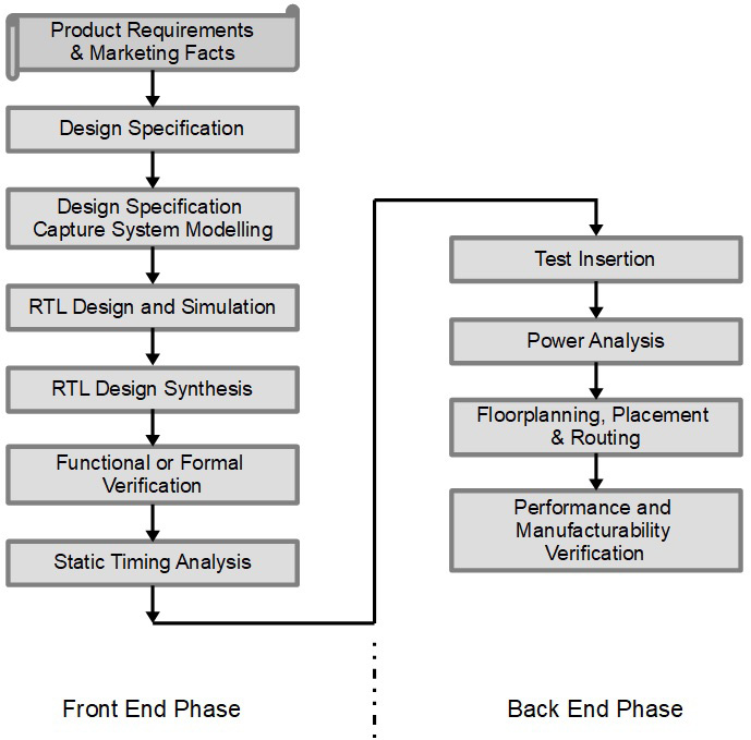
This is the first design step of an SoC, and it consists of capturing the SoC’s specification, partitioning the HW/SW, and selecting the IPs. The design capture could simply be in a text format as an architecture specification document or could be associated with a design capture of the specification in a computer language such as C, C++, SystemC, or SystemVerilog. This design capture isn’t necessarily a full SoC system model – it could just be an overall description of the main algorithms and inter-block IPC. However, we can observe the emergence of the usage of full SoC system models by using different environments and fulfilling a diverse set of reasons. Time to market is becoming more of a challenge for many companies that use ASICs because they have to wait for the silicon to be designed and produced, tested, and then assembled with other components on a board to start the software development process. This can take up to a year, assuming that everything runs smoothly. Companies typically use a virtual prototype (VP) to help them shorten the system design cycle by around 6 months. Building this VP has an engineering cost and requires many technical skillsets with a need for a deep knowledge of the hardware’s architecture and microarchitecture. The following diagram provides an overview of the SoC in ASICs design flow:

Figure 1.11 – The SoC in ASICs high-level design flow
RTL design
The design capture is followed by the RTL design of the SoC components in an HDL language such as Verilog or VHDL. Then, they are assembled at the top-level module of the SoC. The RTL is then simulated using test benches written specifically to verify the functional correctness – that is, the intended functionality – of the RTL design.
RTL synthesis
Once the RTL design has been completed at a specific module level and simulated using the module verification approach, it is synthesized using a synthesis tool. This step automatically generates a generic gate description from the RTL description. The synthesis tool performs logic optimization for speed and area, which can be guided by the designer via specific scripts or constraints files that are provided alongside the RTL files to the synthesis engine. This step performs state machine decomposition, datapath optimization, and power optimization. Following the extraction and optimization processes, the synthesis tool translates the generic gate-level description into a netlist using a target library. The target library is specific to the ASIC technology process node and foundry.
Functional or formal verification
Following the synthesis step and generating a design netlist, a functional or formal verification step is performed to make sure that there are no residual HDL ambiguities that caused the synthesis tool to produce an incorrect netlist. This step involves rerunning functional verification on the gate-level netlist. Usually, two formal verifications need to be run: model checking, which proves that certain assertions are true, and equivalence checking, which compares two design descriptions.
Static timing analysis
This step verifies the design’s timing constraints. It uses a gate delay and routing information to check all the timing paths connecting the logic elements. This requires timing information for any of the IP blocks that are instantiated in the design, such as memories. This analysis will evaluate the timing violations, such as setup and hold times. To ignore any paths or violations forming a special case, the designer can use specific timing constraints to highlight these to the timing analysis tools. This analysis produces a set of results that, for example, report the slack time. The designer uses this information to resynthesize the circuit or redesign it to improve the timing delays in the critical paths.
Test insertion
In this step, various design for test (DFT) features are inserted. The DFT allows the device to be tested using automated test equipment (ATE) when the chip is back from the foundry. It consists of many scan-enabled flip-flops and scan chains. There are also built-in self-test (BIST) blocks memory built-in self-test (MBIST) blocks, which can apply many testing algorithms to verify the correct functionality of the memories. The Boundary-Scan/JTAG is also added to enable board/system-level testing.
Power analysis
Power analysis tools are used to evaluate the power consumption of the ASIC device. These analyses are statistical and use load models that translate into activity factors for the power consumption estimation.
Floorplanning, placement, and routing
The next step opens the backend flow, where the synthesized RTL design undergoes floorplanning, placement, routing, and clock insertion.
Performance and manufacturability verification
Performance and manufacturability verification is the last step of the SoC ASIC design flow. Here, the physical view of the design is extracted. Then, the design undergoes a timing verification process, signal integrity, and design rule checking, which completes the backend design flow.


